
 |

|
| ActiveWin: Reviews | Active Network | New Reviews | Old Reviews | Interviews |Mailing List | Forums |
|
|
|
|
|
DirectX |
|
ActiveMac |
|
Downloads |
|
Forums |
|
Interviews |
|
News |
|
MS Games & Hardware |
|
Reviews |
|
Support Center |
|
Windows 2000 |
|
Windows Me |
|
Windows Server 2003 |
|
Windows Vista |
|
Windows XP |
|
|
|
|
|
|
|
News Centers |
|
Windows/Microsoft |
|
DVD |
|
Apple/Mac |
|
Xbox |
|
News Search |
|
|
|
|
|
|
|
ActiveXBox |
|
Xbox News |
|
Box Shots |
|
Inside The Xbox |
|
Released Titles |
|
Announced Titles |
|
Screenshots/Videos |
|
History Of The Xbox |
|
Links |
|
Forum |
|
FAQ |
|
|
|
|
|
|
|
Windows XP |
|
Introduction |
|
System Requirements |
|
Home Features |
|
Pro Features |
|
Upgrade Checklists |
|
History |
|
FAQ |
|
Links |
|
TopTechTips |
|
|
|
|
|
|
|
FAQ's |
|
Windows Vista |
|
Windows 98/98 SE |
|
Windows 2000 |
|
Windows Me |
|
Windows Server 2002 |
|
Windows "Whistler" XP |
|
Windows CE |
|
Internet Explorer 6 |
|
Internet Explorer 5 |
|
Xbox |
|
Xbox 360 |
|
DirectX |
|
DVD's |
|
|
|
|
|
|
|
TopTechTips |
|
Registry Tips |
|
Windows 95/98 |
|
Windows 2000 |
|
Internet Explorer 5 |
|
Program Tips |
|
Easter Eggs |
|
Hardware |
|
DVD |
|
|
|
|
|
|
|
ActiveDVD |
|
DVD News |
|
DVD Forum |
|
Glossary |
|
Tips |
|
Articles |
|
Reviews |
|
News Archive |
|
Links |
|
Drivers |
|
|
|
|
|
|
|
Latest Reviews |
|
Xbox/Games |
|
Fallout 3 |
|
|
|
Applications |
|
Windows Server 2008 R2 |
|
Windows 7 |
|
|
|
Hardware |
|
iPod Touch 32GB |
|
|
|
|
|
|
|
Latest Interviews |
|
Steve Ballmer |
|
Jim Allchin |
|
|
|
|
|
|
|
Site News/Info |
|
About This Site |
|
Affiliates |
|
Contact Us |
|
Default Home Page |
|
Link To Us |
|
Links |
|
News Archive |
|
Site Search |
|
Awards |
|
|
|
|
|
|
|
Credits |

|
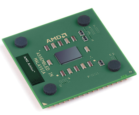
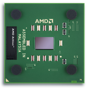
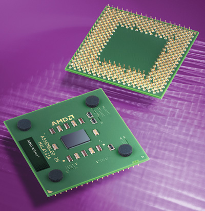
Product: Athlon XP 2200+ |
AMD Athlon XP 2200+ Overview
| Table Of Contents |
| 1:
Introduction 2: CPU Overview & Overclocking 3: Synthetic Benchmarks 4: Games Benchmarks 5: Applications Benchmarks 6: Conclusion |
 With
the recent extreme frequency increase Pentium
With
the recent extreme frequency increase Pentium
That�s
why AMD�s engineers have designed a brand new CPU core, known as
Thoroughbred, that is engraved in
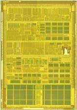
AMD Thorougbred Die
In
reality, the main advantage of the
AMD Athlon XP 2200+ CPU
Despite
its name, the AMD Athlon XP
Apart
from the finer engraving process and the frequency increase; this Athlon
�T-bred� built on the K7 architecture has nothing new in terms of 32-bit
instructions and still hosts
Physically the processor still uses the old good Socket A and doesn�t differ from previous Athlon XP except for the presence of more bridges. The core also looks rectangular while it was looking more like a square before. The Socket A architecture means you�ll be able to use the processor with every Athlon XP Slot A compatible motherboard (most motherboards will require a BIOS update).
CPU Architecture
The Athlon XP
Overclocking
This is probably the most surprising thing for an AMD processor, but the
Athlon XP
AMD Athlon XP 2200+ 0.13�